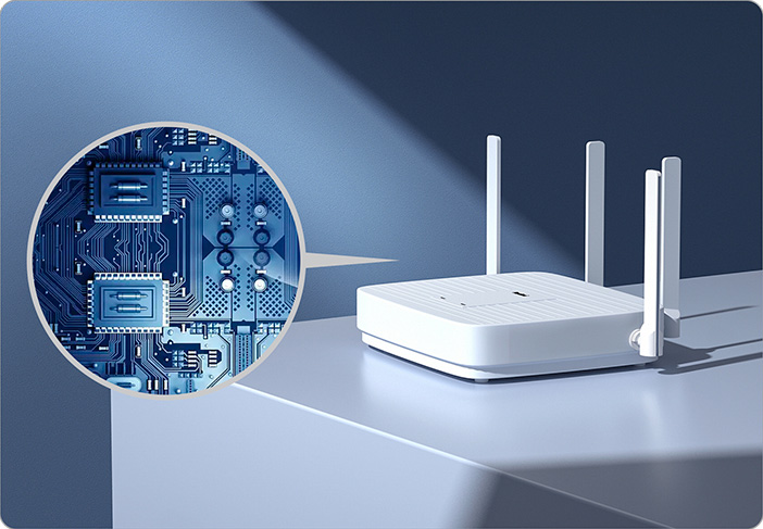
PCBs for Network
Routers
| Thickness | 1.0±0.10mm |
|---|---|
| Material | FR-4 |
| Layers | 4 |
| Min Hole Diameter | ¢ 0.2mm |
| Wire Width | 0.1mm |
| Wire Pitch | 0.1mm |
| Impedance Requirements | 55.0+/-5 Ω |
| Surface Finish | OSP |

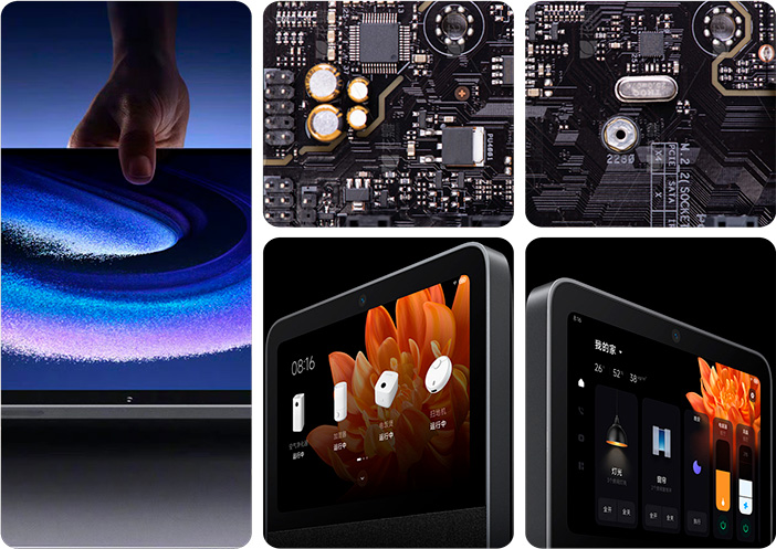
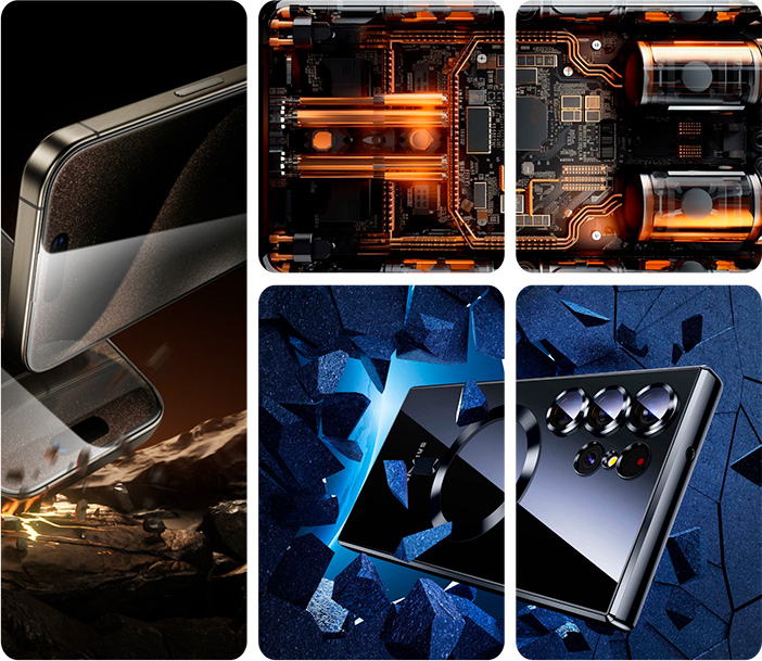
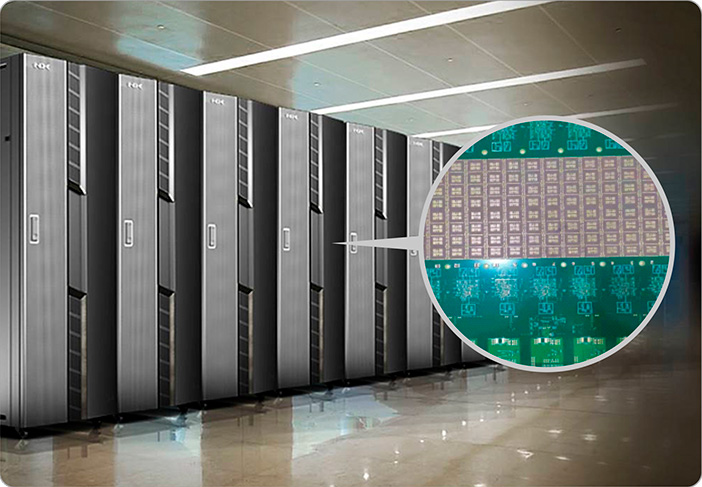
These advanced chips,
optimized for PCB integration,
deliver unparalleled computing power and energy efficiency,
driving innovation in high-tech electronics.

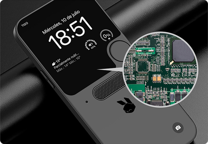
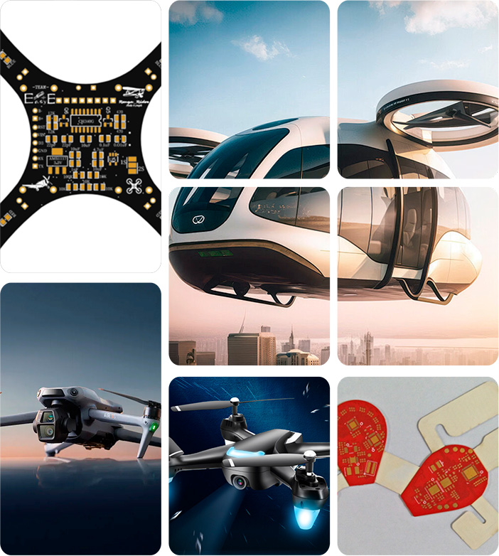
These PCB-integrated routers, tablets,
and computers deliver superior performance,
stable connectivity, and intelligent computing,
empowering diverse electronic applications in the PCB industry.
| Thickness | 1.0±0.10mm |
|---|---|
| Material | FR-4 |
| Layers | 4 |
| Min Hole Diameter | ¢ 0.2mm |
| Wire Width | 0.1mm |
| Wire Pitch | 0.1mm |
| Impedance Requirements | 55.0+/-5 Ω |
| Surface Finish | OSP |

| Thickness | 1.6+0.16mm |
|---|---|
| Material | FR-4 |
| Layers | 6 |
| Min Hole Diameter | ¢ 0.2mm |
| Wire Width | 0.1mm |
| Wire Pitch | 0.075mm |
| Impedance Requirements | 55±5Ω |
| Surface Finish | ENIG |
| Thickness | 1.6+0.16mm |
|---|---|
| Material | FR-4 |
| Layers | 6 |
| Min Hole Diameter | ¢ 0.2mm |
| Wire Width | 0.1mm |
| Wire Pitch | 0.075mm |
| Impedance Requirements | 55±5Ω |
| Surface Finish | ENIG |
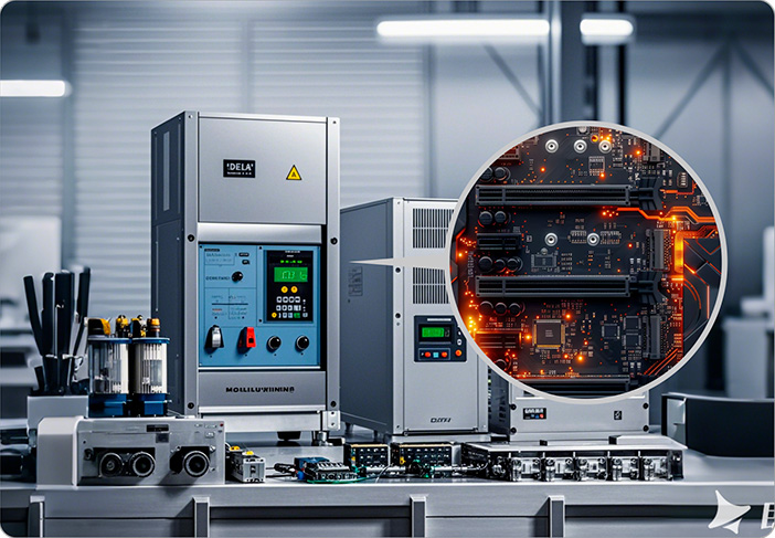
In the PCB industry, the Q91-1250V2 equipment,
with its innovative design, brings efficient
and precise solutions for circuit board processing,
empowering enterprises to improve production efficiency
and demonstrating strong capabilities in high-end PCB manufacturing.
| Thickness | 1.0+0.10mm |
|---|---|
| Material | FR-4 |
| Layers | 6 |
| Half-hole design | ¢ 0.5mm |
| Min Hole Diameter | ¢ 0.2mm |
| Wire Width | 0.075mm |
| Wire Pitch | 0.075mm |
| Surface Finish | OSP |
| Thickness | 1.2+0.12mm |
|---|---|
| Material | FR-4 |
| Layers | 4 |
| Golden Finger | 30uin |
| Min Hole Diameter | ¢ 0.25mm |
| Wire Width | 0.1mm |
| Wire Pitch | 0.1mm |
| Surface Finish | ENIG |
| Thickness | 1.6+0.16mm |
|---|---|
| Material | FR-4 Tq170 |
| Layers | 10 |
| Min Hole Diameter | ¢ 0.25mm |
| copper thickness | 210um |
| Surface Finish | ENIG |
| technical | 1+4+1 |
|---|---|
| Mechanical Through Hole | L1-L6 L2-L5 |
| laser | L1-L2 L5-L6 |
| Thickness | 0.8mm |
| Material | FR-4 Tg170 |
| Wire Width | 0.1mm |
| Wire Pitch | 0.075mm |
| Min Hole Diameter | ¢ 0.1mm(laser) ¢0.3 mm(Mechanical) |
| Surface Finish | ENIG |
| technical | 2+6+2 |
|---|---|
| Mechanical Through Hole | L1-L8 L2-L7 L3-L6 |
| laser | L1-L2 L2-L3 L6-L7 L7-L8 |
| Thickness | 1mm |
| Material | FR-4 highTG |
| Wire Width | 0.075mm |
| Wire Pitch | 0.075mm |
| Min Hole Diameter | ¢ 0.1mm(laser)
¢ 0.25mm(Mechanical) |
| Surface Finish | ENIG + OSP |
| BGA Size | 0.25mm |
| SMD Size | 0.4mm |
In PCB production scenarios,
this AGV robot enables automated material transportation
with intelligent navigation and flexible operation,
reducing costs and improving efficiency for PCB workshops
and facilitating intelligent manufacturing upgrading.
| Layers | 8 |
|---|---|
| Mechanical Through Hole | L1-L8 |
| laser | L1-L2 & L7-L8 |
| Thickness | 1mm |
| Material | Plolyimide+FR4 |
| Wire Width | 0.075mm |
| Wire Pitch | 0.075mm |
| Min Hole Diameter | ¢ 0.1mm(laser)
¢ 0.25mm(Mechanical) |
| Surface Finish | ENIG |
| BGA Size | 0.25mm |
| SMD Size | 0.4mm |
| Layers | 26 |
|---|---|
| Mechanical Through Hole | L1-L26 |
| Thickness | 4mm |
| Material | FR-4 highTG |
| Wire Width | 0.1mm |
| Wire Pitch | 0.1mm |
| Min Hole Diameter | ¢ 0.35mm |
| Surface Finish | ENIG |
| BGA Size | 4mm |
| SMD Size | 0.35mm |

Email: info@safepcbglobal.com
Phone: 626-736-0685
Address: 555 Parkcenter Dr. Ste 200, Santa Ana, CA 92705